在芯片表面使用聚焦离子束形成导电孔及导电垫子,再利用特殊接合方式使导电垫子连接金属导线,以形成导电路径。
iST 宜特能为你做什么
To Reduce Parasitic Resistance With Long Wiring Requirement
To Measure The Internal Nodes Of Your Chip More Easier低电阻联机
以1000um 联机为例,传统FIB联机的电阻为7000ohm(PT);使用宜特N-FIB在芯片表面上联机的电阻约仅10 ohm,这是传统FIB无法做到的。
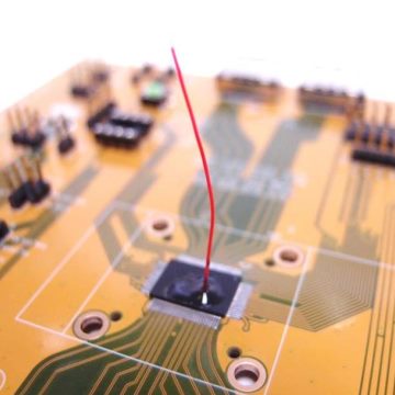
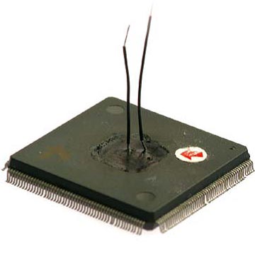
信号引出
利用N-FIB技术将信号藉由银导线引出到芯片外部, 芯片设计者可直接用外部银线加以量测,整个联机路径的电阻、电感较使用探针小而且稳定度较高,并可重复使用。
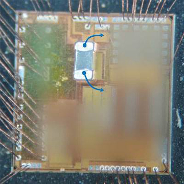
可加入被动组件
利用宜特N-FIB可以在芯片表面加入多种规格的电阻、电容, 让芯片设计者使用此种应用,在设计除错的工作上更加得心应手。

iST 宜特服务优势
| 优势比较 | N-FIB | 传统 FIB |
|---|---|---|
| R esistance with long wiring (1000 μ m) | 1 Ω± 10% | 7000 Ω± 10% |
| Parasitic capacitance | < 200fF | Less |
| Parasitic inductance | ~0.5nH/mm | Less |
| Current limit | Less | Possible |
| Power line | 1A | 3mA |
| Insert device | Yes | No |
案例分享
- 低阻抗的长距离端点连结
- 减少离子束的破坏
- 适用于大电流或电源电路
- 可插入电阻/电容被动组件